Dutch semiconductor equipment manufacturer ASML has revealed a major ASML EUV breakthrough that could transform global chip manufacturing . By enhancing the power of its extreme ultraviolet (EUV) light source, the company expects to increase semiconductor production by up to 50% by the end of the decade . This technological leap promises to lower manufacturing costs while addressing the surging demand for advanced processors driven by artificial intelligence .
The new method elevates the EUV light source output from the current 600 watts to a staggering 1,000 watts . According to Teun van Gogh, the executive vice president overseeing ASML’s NXE line, this power upgrade will allow clients to process roughly 330 silicon wafers per hour by 2030 . That is a significant jump from the approximately 220 wafers per hour achieved by today’s leading systems, offering chipmakers a crucial advantage in a highly competitive market .
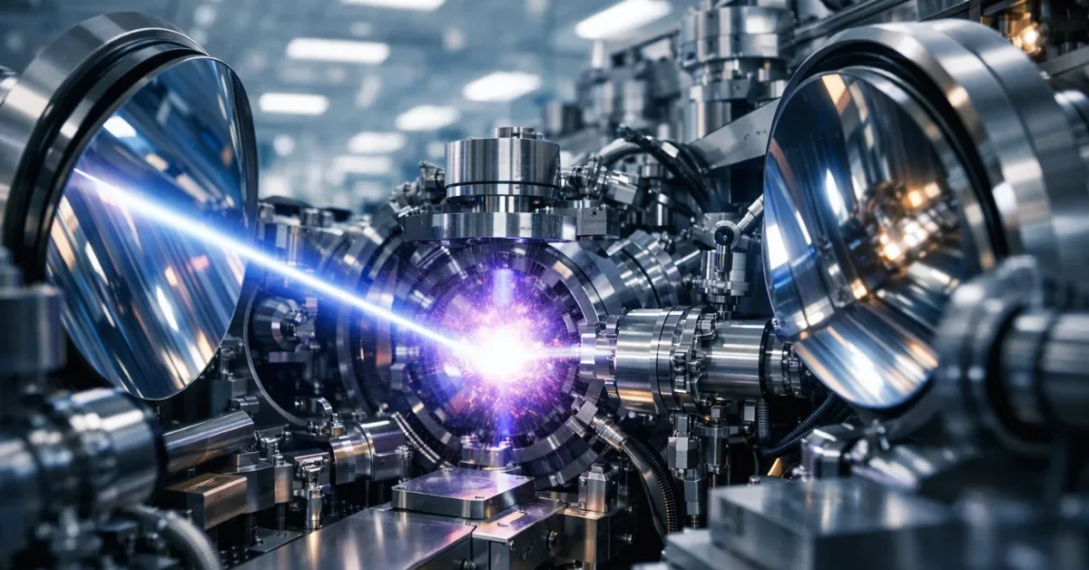
How the Upgraded Light Source Works
The core benefit of this upgrade is efficiency . Manufacturing microchips is comparable to developing a photograph . In a semiconductor fabrication plant, EUV light is projected onto a silicon wafer that has been coated with a light-sensitive chemical called photoresist . By intensifying the EUV light source, the necessary exposure time for each layer of the chip is significantly shortened . This accelerated exposure allows chipmakers to increase their throughput, which ultimately reduces the manufacturing cost per individual chip .
To generate the extreme ultraviolet light, ASML machines propel a steady stream of molten tin droplets through a specialized chamber . The company achieved the new 1,000-watt milestone by doubling the frequency of these droplets to approximately 100,000 per second . Inside the chamber, a powerful carbon dioxide laser blasts the tin . Instead of the traditional single shaping burst, the updated method utilizes two smaller laser bursts to vaporize the tin and convert it into a glowing plasma .
This plasma reaction reaches extreme temperatures that are hotter than the surface of the sun . During this intense process, the plasma emits light at a specific 13.5-nanometer wavelength . This light is captured and reflected using highly complex precision optical systems supplied by Germany’s Carl Zeiss AG . These optics route the light with perfect accuracy back into the machine to pattern the intricate transistor designs onto the silicon .
System Upgrades and Future Platforms
Deploying this massive increase in power presents unique integration challenges . ASML traditionally offers Productivity Enhancement Packages to its clients, allowing semiconductor fabrication plants to upgrade their existing tools without purchasing entirely new lithography machines . However, retrofitting older equipment is not always feasible . Previous generation systems, such as the NXE:3400C and NXE:3400D models, have strict thermal limits that restrict them from handling a 1,000-watt source . Consequently, this advanced light source approach will be targeted primarily at existing NXE:3800E systems and the highly anticipated, next-generation High-NA EXE:5000 and EXE:5200 platforms .
ASML does not plan to stop at 1,000 watts . Company leaders believe the techniques used to achieve this current breakthrough will pave the way for even more profound performance enhancements . ASML has already set its sights on pushing future light source power levels to 1,500 watts, with an ultimate goal of reaching 2,000 watts to continually improve global production capabilities .
Financial Growth and Market Competition
This technological leap arrives as the semiconductor industry experiences a massive surge driven by artificial intelligence . Advanced chips featuring nanotechnology are the critical foundation for AI hardware, powering the large language models that are rapidly transforming the tech sector . To meet this demand, top memory manufacturers like Micron are already utilizing ASML’s EUV lithography systems at the 1γ node to efficiently produce advanced DRAM and NAND chips .
ASML’s financial health reflects this insatiable market demand . The company concluded 2025 with $39.16 billion in net sales and a net income of $11.5 billion . A particularly strong fourth quarter brought in $11.62 billion in revenue, leaving the company with a massive $46.47 billion order backlog . Looking ahead, management projects 2026 net sales to range between $40.72 billion and $46.7 billion . Showcasing confidence in their ongoing expansion, ASML authorized a $14.37 billion share repurchase program . Over the past twelve months, the company’s stock value has climbed by 101 percent .
Despite operating as a monopoly in the EUV lithography sector, ASML is working to aggressively defend its territory . At least two startup companies based in the United States, Substrate and xLight, have recently raised hundreds of millions of dollars to engineer American-made alternatives to ASML’s machinery . By continually advancing the most technically difficult component of the EUV process, ASML aims to widen its competitive lead and secure its dominance in the semiconductor supply chain .
